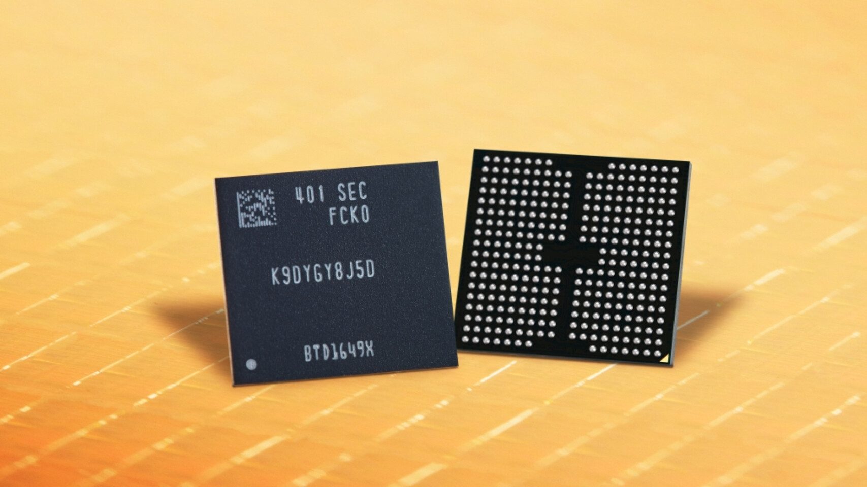
Samsung is moving closer to its long-term 1,000-layer NAND goal by taking a different route than a single ultra-thick chip. Instead, Samsung Stacks Two 450-Layer V-NAND chips together using advanced packaging, creating a bonded 900-layer design that pushes the company’s flash roadmap forward without waiting for one monolithic die to do all the work.
How Samsung is reaching 900 layers
The reported approach uses Cell Multi-Bonding, or CMB, which is Samsung’s version of wafer stacking through hybrid bonding. In practical terms, that means two silicon wafers are permanently fused together with embedded metal bumps, creating what functions like a single chip.
This is not just a simple stacking trick. Samsung is trying to connect two full chip backsides, which is a more complex process than the packaging used in many other NAND designs. The result is a way to extend layer counts while keeping the manufacturing challenge more manageable than building one much taller chip.
Why 450-layer NAND is already hard to work with
Stacking wafers at this scale brings its own problems. One of the biggest is warping, which becomes more difficult to control as NAND designs get thicker. Samsung has reportedly addressed that with microscopic chucks and updated bonding methods designed to reduce alignment and overlay errors during the stacking process.
Samsung has also made internal changes to the NAND itself, including new bitline and wordline structures. Those changes are meant to help keep power use in check while avoiding chips that become too large to manufacture efficiently.
- Two 450-layer V-NAND chips are being bonded into a 900-layer design
- The process uses Samsung’s Cell Multi-Bonding technology
- Microscopic chucks help manage wafer warping during bonding
- New bitline and wordline structures are aimed at power and chip-size efficiency
Where this fits in Samsung’s NAND roadmap
Samsung first introduced its 10th-generation V-NAND last year, bringing the company above 400 layers on a single module and adding hybrid bonding for the first time. This latest step suggests that the technology has continued to mature, but the company still appears to be relying on a staged rollout rather than jumping straight to a 1,000-layer part.
The current plan seems to be mass production of the 10th-generation V-NAND first, followed by the bonded 900-layer design. High-volume production of the new stacked chip is still said to be a few quarters away, so availability is not immediate.
Why the record matters
At the moment, SK hynix holds the volume-production record with its 321-layer 4D NAND design. Samsung’s 900-layer approach is clearly aimed at taking that crown, at least on paper, while also building a path toward 1,000-layer NAND by 2030.
For readers following storage hardware, the bigger takeaway is that NAND scaling is becoming as much about packaging and bonding as it is about raw layer counts. Samsung’s latest move shows how far flash development has shifted from simple node progression to more advanced chip assembly techniques.
Source
Source: TechPowerUp