AMD’s next big CPU jump is already taking shape behind the scenes, and the latest report points to a major manufacturing shift for Zen 7. The architecture is said to be lined up for TSMC’s A14 process, while AMD also appears to be looking at more advanced packaging options as it plans how to build out future desktop and server chips.
What the report says
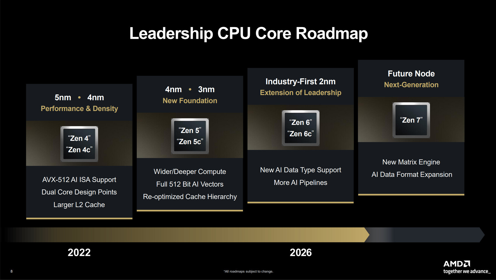
AMD is still preparing its Zen 6 generation under the EPYC Venice server family, but development work on Zen 7 is reportedly moving forward as well. Taiwanese outlet Commercial Times says AMD is considering TSMC’s A14 node for Zen 7, which would put it on the first angstrom-era manufacturing process.
That would follow AMD’s recent move to ramp EPYC Venice on TSMC’s 2 nm node for Zen 6. Zen 7 is expected to push further on both efficiency and performance, especially if it ends up using the newer A14 process.
Architecture changes AMD is reportedly lining up
The Zen 7 CCD IP is said to carry the codename Grimlock. The report suggests AMD wants the design to be more AI-friendly, with better use of the 16 CPU cores per CCD for future workloads.
Several instruction set additions are mentioned for Zen 7:
- AVX10, which combines AVX-512 and AVX2 features for better compatibility and performance in vector-heavy workloads
- ACE or Advanced Matrix Extensions for Matrix Manipulation, a matrix math instruction set that could span devices from smartphones to servers
- FRED or Flexible Return and Event Delivery, which replaces the current interrupt model to help reduce latency
- ChkTag x86 Memory Tagging, aimed at reducing risks tied to buffer overflows and use-after-free bugs
For buyers and enthusiasts, the practical takeaway is that AMD appears to be building Zen 7 with broader compute workloads in mind, not just traditional CPU throughput.
Packaging could be part of the story, too
The report also says AMD is evaluating more advanced packaging technologies, including next-generation 3D V-Cache. Another option under consideration is Powertech’s FOPLP, or Fan-Out Panel-Level Packaging.
Powertech is a Taiwan-based packaging vendor and one of the larger OSAT players. If AMD chooses to work with it, that could point to a wider effort to diversify packaging supply rather than relying so heavily on TSMC alone.
What remains unclear
The biggest unknown is how much of this will carry through to final products. The report does not confirm a final node choice, final packaging stack, or a launch timeframe for Zen 7.
For now, the main takeaway is that AMD is reportedly aiming for a much more advanced platform on both the manufacturing and architecture sides, with Zen 7 positioned as a meaningful step beyond Zen 6.
Source
Source: TechPowerUp